3D printing process connects optical microchips
Communication with light is rapidly gaining in importance in view of constantly increasing data traffic. Photonics is currently facing the challenge of miniaturizing components and assembling them into compact and powerful integrated systems that are suitable for a wide range of applications from information and communication technology to metrology, sensors and medical technology.
Of particular interest in this context are hybrid systems that combine a large number of optical components with different functions. These hybrid systems offer decisive advantages in terms of performance and design freedom compared to monolithic integration concepts in which all components are realized on one chip. For example, hybrid integration allows all components to be individually optimized and tested before they are combined into a more complex system. Up to now, however, the construction of optical hybrid systems has required complex and expensive methods to precisely position the components in relation to each other and to connect the optical interfaces to each other with low loss.
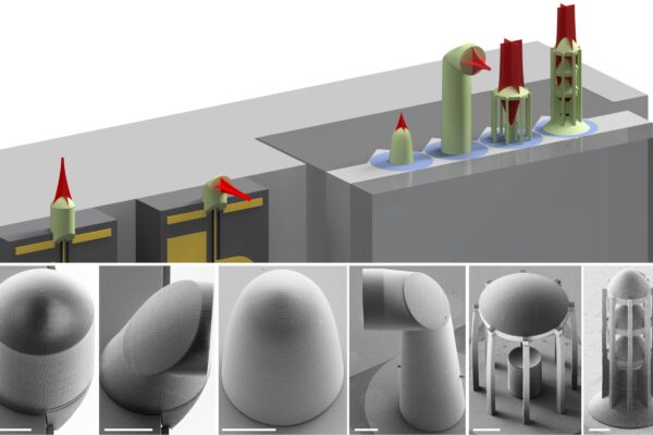
KIT scientists have now found a new solution for coupling optical microchips to each other or to optical fibers: They use tiny beam-forming elements that can be applied directly to the facets of optical components using a high-precision 3D printing process. These elements can be manufactured in almost any three-dimensional shape and thus allow a wide variety of optical components to be combined with low losses and high positioning tolerances.
The researchers use multiphoton lithography to produce the three-dimensional elements: an ultrashort pulse laser writes the specified structures layer by layer into a photoresist that cures afterwards. This makes it possible to print 3D structures the size of just a few hundred nanometers. In addition to microlenses, other optical free-form elements such as micro mirrors can also be created with this process in order to adapt beam shape and direction of propagation simultaneously. In addition, complete multi-lens systems for beam expansion can be produced, which can be used to increase the positioning tolerance during component assembly.
The researchers validated their concept in several experiments. They produced the micrometer-sized beam-forming elements in various shapes and tested them on a variety of chip and fiber facets.
As reported by the scientists in the journal Nature Photonics, they achieved coupling efficiencies of up to 88 percent between an indium phosphide laser and an optical fiber. The experiments were conducted at the Institute of Microstructure Technology (IMT), the Institute of Photonics and Quantum Electronics (IPQ) and the Institute of Automation and Applied Computer Science (IAI) of KIT in cooperation with the Fraunhofer Institute for Telecommunications (Heinrich Hertz Institute, HHI) in Berlin and IBM Research in Zurich. The technology is currently being transferred to industrial applications by KIT spin-off Vanguard Photonics.
“Our concept paves the way for the automated and thus cost-efficient production of high-performance and versatile optical hybrid systems,” explains Professor Christian Koos, head of IPQ and member of the IMT management team and co-founder of Vanguard Photonics. “It thus makes a decisive contribution to unlocking the enormous potential of integrated optics in industrial applications.”
Related articles:
World’s first switchable quantum metamaterial investigated
Silicon photonics on verge of ‘massive growth,’ says report
 If you enjoyed this article, you will like the following ones: don't miss them by subscribing to :