Ultra-low power microcontrollers enabling energy harvesting applications
One of the first technologies to come to fruition from this programme is a new semiconductor process technology that will allow the development of a whole range of new ultra-low power semiconductor devices.
This process is known as Silicon on Thin Buried Oxide (SOTB). It was derived from the Fully Depleted – Silicon on Isolator (FD-SOI) process technology that is commonly used to manufacture high performance System on Chip (SOC) and Application Specific Standard Products (ASSPs) today. Devices using FD-SOI process technology tend to offer high levels of integration and high clock rates. However, while they can offer impressive figures for Icc/MHz they are not normally considered to be low power and generally cannot integrate embedded memory.
Silicon on Thin Buried Oxide (SOTB) has been specifically developed to support the design of the next generation of ultra-low power embedded microcontrollers, aimed at providing high performance solutions for energy harvesting applications.
Embedded controllers implemented on the new SOTB process will be able to combine high CPU performance, high levels of memory integration, and extremely low levels of both active and standby current. This makes them ideal for connected applications that will harvest their energy from the environment.
Most of today’s microcontrollers are developed using one of the many varieties of CMOS bulk silicon processes. These processes have a long history in the semiconductor industry and are extremely well understood, both in terms of the benefits of these specific processes and their weaknesses. When we want to develop a new microcontroller for a specific application, we must choose the process carefully, depending on the exact electrical characteristics of the device we require.
Figure 1 shows a comparison between SOTB and many of the various processes used to implement microcontrollers available today, at various process geometries.
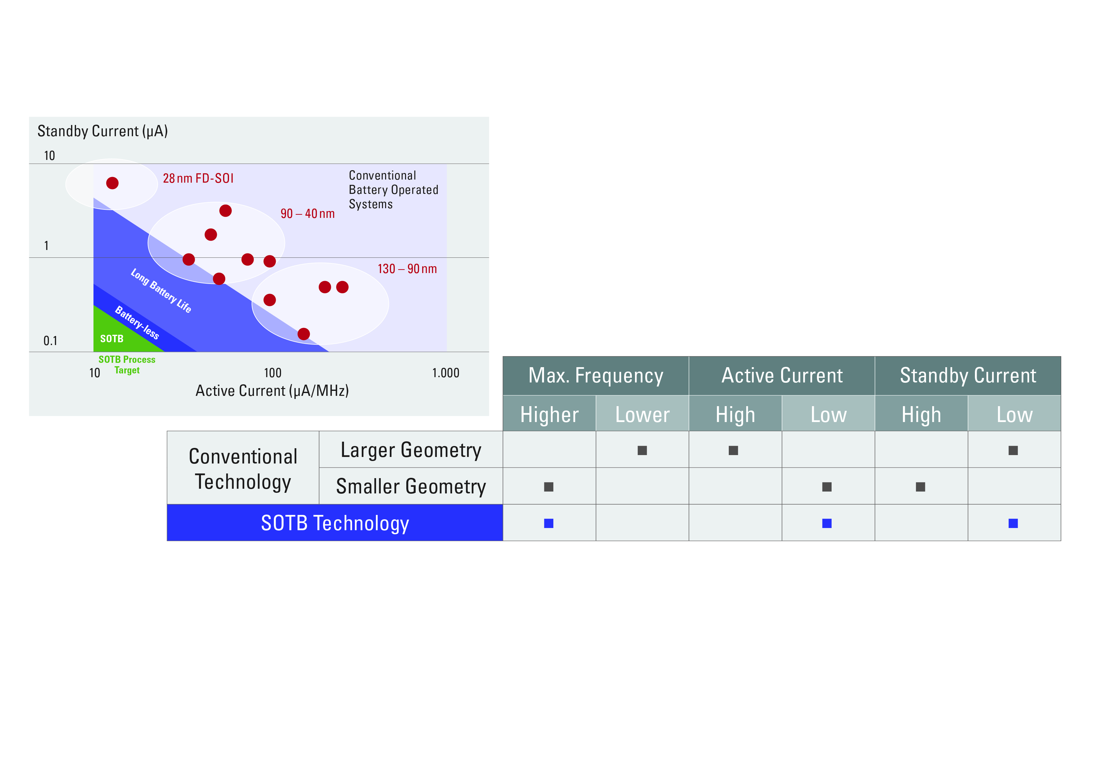
We can choose to use an advanced process node, typically with a line width of 40 nm or the even smaller widths available today. Here we have the advantage of being able to offer products with high levels of peripheral integration, including large on-chip flash memories of over 2 Mbytes, along with high clock rates. Operation in excess of 200 MHz is not uncommon for such a process. However, while the active switching current of such a process is typically very low at around 50 – 100 µA/MHz, the leakage current from each gate in such a small process width is very high. This results in extremely high standby currents, typically 10 – 100 µA or more.
For many applications, especially those that use a battery or require energy harvesting techniques, lower leakage is probably the most important parameter at such low current standby modes. If this is the key requirement for the design, we typically have to choose a process with a larger line width. This restricts these modules in terms of both the performance and the level of integration of memory and other peripherals. Clock rates of less than 80 MHz are typical with memory sizes normally restricted to less than 512 Kbytes.
Typically, these processes may have active modes with current consumption in the range of 250 – 500 µA/MHz, while the leakage currents can be in the range of a few hundred nA.
The new SOTB process can now offer active mode current of less than 20 µA/MHz and leakage currents down to 150 nA, while still allowing the development of devices with reasonably high clock rates, large embedded flash memories and SRAMs on chip.
This combination of integration and power consumption will make devices developed on this process ideal for energy harvesting applications. It is also likely to reduce the overall energy demands by up to 10 times compared to a device using the traditional CMOS bulk silicon process.
One of the huge breakthroughs in the development of this technology has been the ability to realise a hybrid silicon structure. As this combines the benefits of the new SOTB process and the existing standard bulk silicon technology on the same design, we can utilise the strengths of both technologies on the same device and provide microcontrollers with embedded flash memory.
The use of the hybrid structure means we can use the new ultra-low power SOTB technology for the gates used in the kernel area. Key logic components such as the CPU and peripherals can be implemented and will use the lowest possible power. We can still use standard bulk silicon gates for features such as the I/O ring and analogue components, where high voltage drive may be required. This means that designers can easily work with these new microcontrollers as they will have similar electrical characteristics to today’s existing microcontrollers.
Figure 2 illustrates this hybrid architecture.

This diagram also shows some of the benefits of the SOTB gate structure. In a traditional CMOS bulk silicon gate design, we must inject channel impurities or dopant atoms into the silicon during the manufacturing process, which enables the gate to conduct when required. The number of atoms injected into each gate is extremely hard to control accurately, so the gate threshold characteristics can vary greatly across a device. This is especially a problem with smaller silicon geometries when the number of atoms involved is extremely small, sometimes in the region of 100 individual atoms. This means that there can be a significant variability in the number of dopant atoms in each gate, resulting in a significant variability in the switching characteristics of each gate within the device.
SOTB avoids this problem by using a dopantless channel design in which the characteristics of the gate are controlled by the extremely thin oxide layer within the gate. Using modern process technology, this is extremely well controlled and is therefore extremely repeatable across the device.
This means that the variation in threshold voltage between each gate is much lower than with the traditional bulk silicon gate design. As will be seen in a moment, this reduction in the variation of the threshold voltage between gates on a SOTB device allows us to greatly reduce the operating voltage and hence the energy used to switch the gate. This limit in the variation of the threshold voltage between the gates on the device also has several other significant benefits, such as a reduction in the noise generated between matched pairs of gates within the device.
The noise reduction also has an impact on the analogue performance of the device. Due to the lower internal noise, the analogue performance is significantly enhanced, allowing the integrated analogue components to provide higher performance than on a standard CMOS bulk silicon design.
The thin Silicon on Isolator (SOI) layer also has some additional benefits, as it provides extra protection from errors causes by cosmic rays. As such, the software error rate on these devices is significantly lower compared to similar devices on the same process node.
Figure 3 illustrates another benefit of the SOTB technology: the ability to apply a negative back bias voltage to each gate. This allows us to manipulate the switching thresholds of each gate on the device, either individually or across the total device.
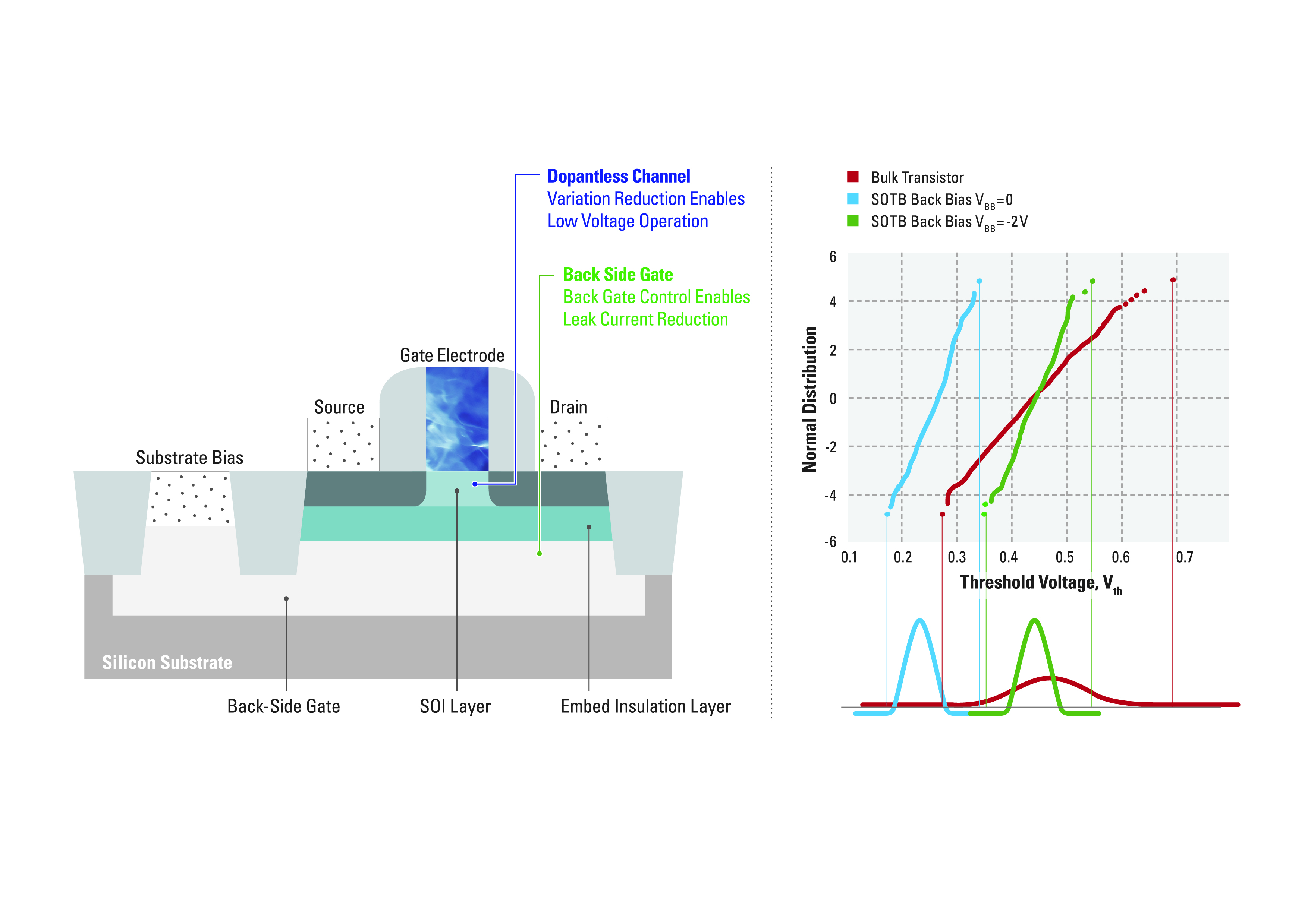
Figure 3 (left) illustrates the design of the SOTB gate with the back-side gate used to control leakage, the SOI layer and the dopantless channel. This enables the reduction in gate variability and so allows for the extremely low active current.
Figure 3 (right) shows a comparison between an SOTB device and a device made on a standard bulk silicon process.
The graph on the left-hand side of Figure 3 shows the threshold voltages for both a standard CMOS bulk gate and an SOTB gate. The red line on this graph shows the range of switching characteristics for a typical device implemented on a bulk silicon process. In this case, we show the variation in switching threshold between the 1 million individual transistors on the test chip. The diagram shows that the best gates will switch at around 0.3v, while due to the inherent variability of the process, the worst gates will switch somewhere in the region of 0.7v. In order to guarantee the operation of every gate on the device, we must therefore operate at voltages significantly above 1.0v. This of course has a direct impact on the power consumed by the module.
The blue line in Figure 4 shows the characteristics of the SOTB gate with the huge reduction in variability and the narrow range of switching characteristics that can be achieved with this process. Devices based on the SOTB process can safely run at much lower voltages and guarantee that every gate will operate correctly, resulting in a huge reduction in the value of the active power consumption.
The green line in Figure 4 shows the result of the back bias being applied. We can control leakage on individual gates. In other words, we can place part or all of the device into an extremely low leakage state, which greatly reduces standby current.
The result of this new process is that we can develop a new generation of microcontroller products. These will combine the best qualities of both smaller geometry technologies with their high levels of integration, low active current and larger geometry, low leakage current devices.
Renesas have now finished development of the first microcontroller using the SOTB process. The use of the SOTB process allows us to produce a device with a unique combination of performance, integration and power consumption. The first device combines a Cortex M0+ Core running at up to 64 MHz with a high level of peripheral integration and up to 1.5 Mbytes of flash and 256 Kbytes of on-chip SRAM.
The use of the Silicon on Thin Buried Oxide technology on this new device has resulted in some unique low power characteristics. The first device has the following features and future devices using this process could offer even lower power consumption.
- Active current of 20 µA /MHz
- Standby Current of 200 nA
- ADC operation 3 µA @ 32 kHz
- 256 Kbyte SRAM with 1 nA / Kbyte standby current
The first device to use the new SOTB process is the Renesas R7F0E017. The block diagram in Figure 4 provides an overview of its features.

The new Renesas R7F0E017, with its unique combination of large on-chip flash memory and on-chip SRAM along with ultra-low power consumption levels, will be ideal for a wide range of applications. These include applications that cannot use a battery or remote power source and energy has to be supplied from the environment.
For the first time, the first SOTB embedded controller will allow powerful, connected applications to source energy from the environment. For this reason, it includes an integrated energy harvesting controller on chip.
This unique peripheral is designed to allow the microcontroller to start from an energy harvesting source and also to manage external rechargeable batteries or super capacitors to provide a power reservoir.
There are many issues that must be resolved when designing an energy harvesting application. For example, one of the biggest problems when using a normal microcontroller is managing the start-up current, as an energy source can normally only supply a small amount of current at any time. Yet a normal microcontroller will typically use significantly more current than is available from the energy source during the start-up phase.
The energy harvesting controller on the R7F0E017 manages this start up current along with the whole start up sequence, so thmicrocontroller starts up reliably and safely.
Figure 5 shows the energy harvesting controller implemented on the R7F0E017.

The R7F0E017 is able to run safely from a pure energy harvesting power source due to the operation of the Energy Harvesting Controller. The device can operate from a wide range of potential energy sources including solar power, vibration, pressure and temperature difference, and many others. The integrated energy harvesting controller, supported by very few inexpensive external components, completely manages the cyclic wake-up sequence of the microcontroller, only using the extremely low energy harvesting source current. The energy harvesting controller includes internal ‘inrush-current’ protection and can operate at very low voltage level to avoid malfunctions during the start-up phase.
The use of Silicon on Thin Buried Oxide technology enables Renesas to provide devices with unique characteristics that make them ideal for applications that harvest energy from the environment. The combination of low power consumption – both in active and standby mode – along with the large on-chip memory and high-performance CPU will allow users to develop powerful solutions for the next generation of applications. This will provide solutions for applications we cannot yet imagine.
Samples of the R7F0E017, along with a complete suite of development tools, will be available to beta customers in early 2019, with general samples available in the second half of 2019.
About the author:
Graeme Clark has been with Renesas Electronics Europe and previously Hitachi Electronics supporting low power microcontrollers in a variety of roles for over 20 years. He is now responsible for the introduction of the new SOTB based embedded controllers into the European market.
 If you enjoyed this article, you will like the following ones: don't miss them by subscribing to :