Power Limit for Insulation Capabilities of Modern IGBT/MOSFET Gate Drivers
In high reliability, high performance applications, like electrical/hybrid vehicles, isolated gate drivers need to ensure the isolation barrier stays intact under all circumstances. The power density of modern power converters/inverters is rising due to the continuous improvement of Si-MOSFET/IGBT and the introduction of GaN and SiC technologies. Therefore, new, highly integrated, isolated, and robust gate drivers are needed. Those drivers provide a small form factor because the electrical isolation is already integrated on the driver chip. This electrical isolation can be performed by means of integrated high voltage microtransformers or capacitors.1, 2, 3 One unpredictable system fault can cause damage to, and the explosion of, power switches or even of the whole power inverter. Therefore, gate driver isolation safety performance needs to be investigated for high power density inverters. The isolation reliability must be tested and validated, in the worst case, when power-switches destruct.
Introduction
An inverter’s bank capacitor of several thousand µF will be rapidly discharged in the worst case, when the high power MOSFET/IGBT fails. The released energy causes MOSFET/IGBT damage, package explosion, and plasma exit into the environment.4 One part of the energy flows into the gate-driver circuit causing electrical overstress.5 Due to extremely high power density, the driver chip should be constructed to maintain electrical isolation even if the chip itself fails.
Construction of Modern, Highly Integrated Gate Drivers
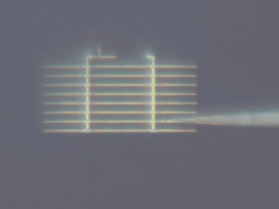
Chip-scale isolation adapts the planar microtransformer approach to provide electrical isolation. It is fabricated using wafer-level techniques and configured in a semiconductor component form-factor.1 An iCoupler® channel consists of two integrated circuits (ICs) combined with chip-scale transformers (Figure 1). An insulation layer provides the isolation barrier to separate the top and bottom coils of each transformer (Figure 2). Digital isolators use a minimum of 20 μm thick polyimide insulating layers between planer transformer coils that are part of the wafer fabrication process. This manufacturing process allows for the isolation elements to be integrated with any foundry semiconductor process at low cost and with excellent quality and reliability. The cross section in Figure 2 shows the turns of the top and bottom coils separated by the thick polyimide layer.

A split lead-frame within the package completes the isolation. When a gate driver output chip is damaged due to a power switch explosion, the internal chip partitioning and arrangement must ensure the isolation layer remains intact. Several protection measures have been implemented to ensure gate driver isolation survival:
- Properly dimensioning the external circuit to limit energy flow into the gate driver chip
- Appropriate placement of output transistors on the driver chip
- Appropriate placement of microtransformer on the chip
- Appropriate arrangement control and driver chip inside of the package

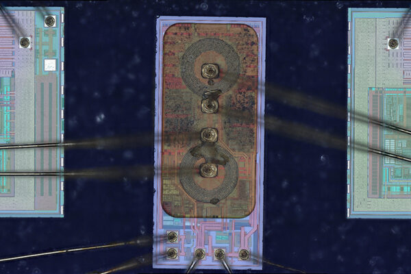
The internal chip arrangement gate driver of ADuM3223 (Figure 1) exhibits one example of chip placement avoiding breakdown of the electrical isolation during extreme electrical overstress.
Destructive Test Simulating Worst Case Inverter Failure
A test circuit with two voltage levels of 385 V and 750 V was built to emulate real power inverter conditions. The voltage level 385 V is very common in a system requiring power factor correction with a 110 V/230 V ac grid. The voltage level of 750 V is common in high power inverters used in drive applications using switches with a rated breakdown voltage of 1200 V.
In the destructive test, one inverter leg, consisting of a power switch and an appropriate driver, was turned on until the switch failed. The waveform during destruction was recorded to determine the energy level flowing into the gate driver chip. Several protection measures were investigated in order to limit the destruction energy flowing into the gate driver circuit. Several types of IGBTs and MOSFETs were used in the destructive tests.
Test Circuit with Controlled MOSFET/IGBT Damage
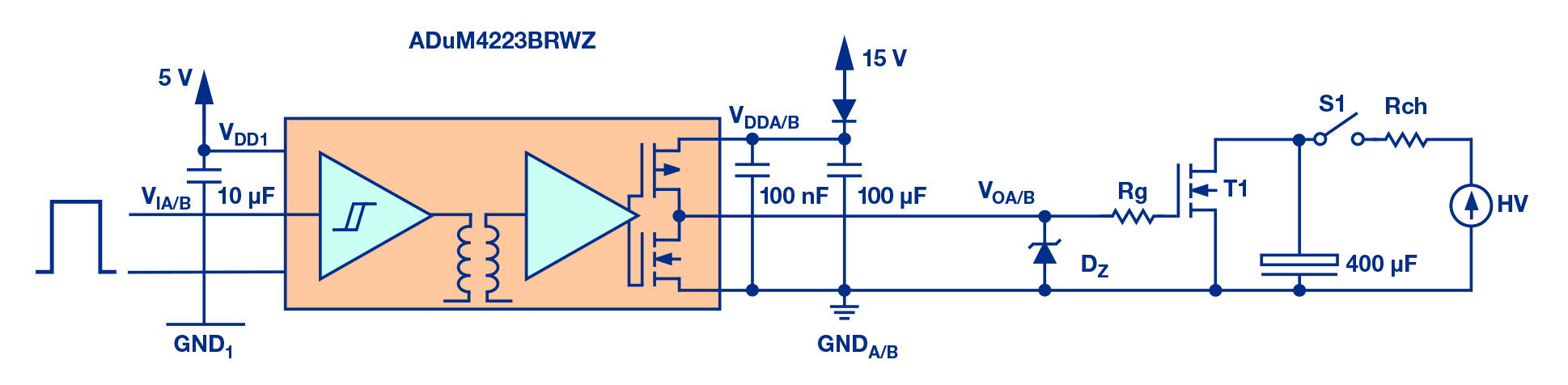
For the IGBT/MOSFET driver electrical overstress tests (EOS-test), a circuit very close to real-world conditions was setup. The circuit included capacitors and resistors reasonable for inverters in the power range of 5 kW to 20 kW. For gate resistor Rg, axial type, 2 W rated power metal resistors were used. One blocking diode, D1, was applied to avoid energy reversing from the high voltage circuit into the external power supply. This also reflected realistic conditions, as floating power supplies include at least one rectifier (that is, bootstrap circuit). The high voltage supply, HV, charged the block electrolyte capacitance by a circuit including a charge resistor, Rch, and one switch, S1.
For the EOS-test, a turn-on signal of 500 µs was applied to control input VIA or VIB. This turn-on signal, which was transmitted via the microisolation, caused a short condition and destruction of the power transistor, T1. In some cases, transistor package explosions were observed.
Four power switch types at two voltage levels were used to simulate inverter damage. The first test for a particular switch type was performed without, and then with, a power limiting circuit. To limit energy flowing into the driver circuit during the damage phase, Zener diode Dz (BZ16, 1.3 W) was applied directly to the driver output pin for some tests. Different values of gate resistors have been investigated as well.
of power switch destruction on isolation withstand.


to the input and output chips.
Test Circuit for Direct Gate Driver Circuit Damage without Energy Limit
Another test simulating the worst-case condition was performed, wherein the destructive energy was applied directly to the input and output chips of the gate driver. During this destructive test, the fully charged bulk capacitor was directly connected to the output pin of the gate driver (Figure 4). This test exhibited the worst possible overstress, and thus examined the isolation withstand capability. The energy flowed directly into the driver circuit while the gate resistor was the only power limiting device. The relay, S2, coupled the high voltage into the gate driver output circuit.
The worst-case test without any devices limiting energy flow into the input and output chips is presented in Figure 5. The direct application of high voltage 750 V via switch S1 into the output chip represents the worst-case condition, when the intermediate high voltage 750 V is directed to the driver chip without an energy limiting gate resistor.
Another possible worst case exhibits the application of excessive supply voltage to the control chip on the primary side of the driver. The maximum recommended input supply voltage is 5.5 V. If the dc-to-dc converter generating input voltage loses regulation, its output voltage could increase. In case of lost regulation, the converter’s output voltage can increase by a factor of two to three for state of the art dc-to-dc converters. Energy applied into the input chip of ADuM4223 is limited and, as always, other devices, like resistors, power switches, and inductors, are in place. Those devices impede the energy flow into the control chip. A supply voltage of 15 V with current limit 1.5 A was chosen for realistic simulation of the dc-to-dc converter malfunction.
Experimental Results
Table 1 presents the result of the overstress tests done using the circuits of Figure 3, Figure 4, and Figure 5. In order to determine the impact of the protection circuit, two tests have been done for each MOSFET/IGBT power switch type. For the worst-case tests of 9, 10, and 11, mechanical switches S1 and S2 were used.


no driver destruction was observed.

the gate driver failed.
In general, the Zener diode helps to protect the driver circuit, as the table states (when comparing test 1 against test 2). However, when the gate resistor value is too small, the driver will be destroyed despite the Zener diode (compare test 3 and test 4).
By comparing test 2 with test 3, and test 3 with test 4, the driver damage energy can be estimated. A very interesting conclusion was provided by tests 5 and 6: super-junction MOSFETs seem to cause significantly lower energy levels flowing into the gate driver than one IGBT having the same power rating. The purpose of tests 9, 10, and 11—with unlimited energy flow into the control and driver chip—was to investigate the isolation withstand performance in worst-case scenarios.
Different Destruction Behavior of a MOSFET vs. an IGBT
The destructive tests showed different waveforms experiencing power switch damage. Figure 6 presents the waveforms for a superjunction MOSFET. The time period between turn-on and chip destruction was approximately 100 µs. Very limited current flowed into the driver chip, which withstood the overstress. For the same test condition, a standard MOSFET caused significantly higher gate current and overvoltage resulting in driver destruction, as presented in Figure 7.
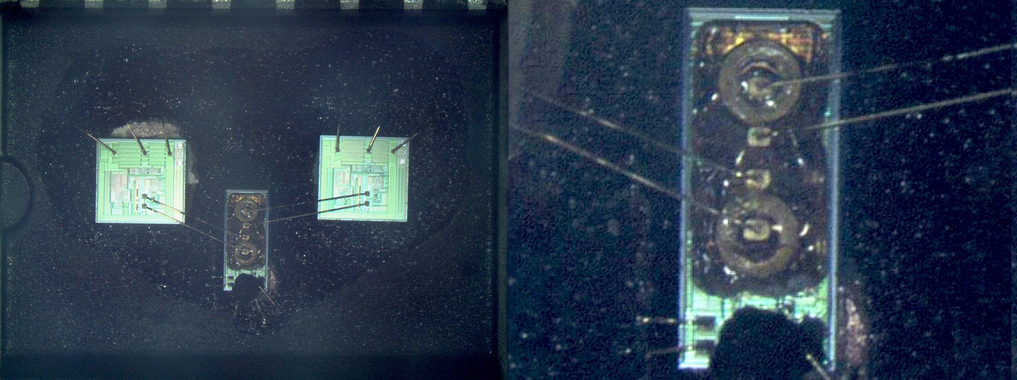
Analysis of Chip Damages
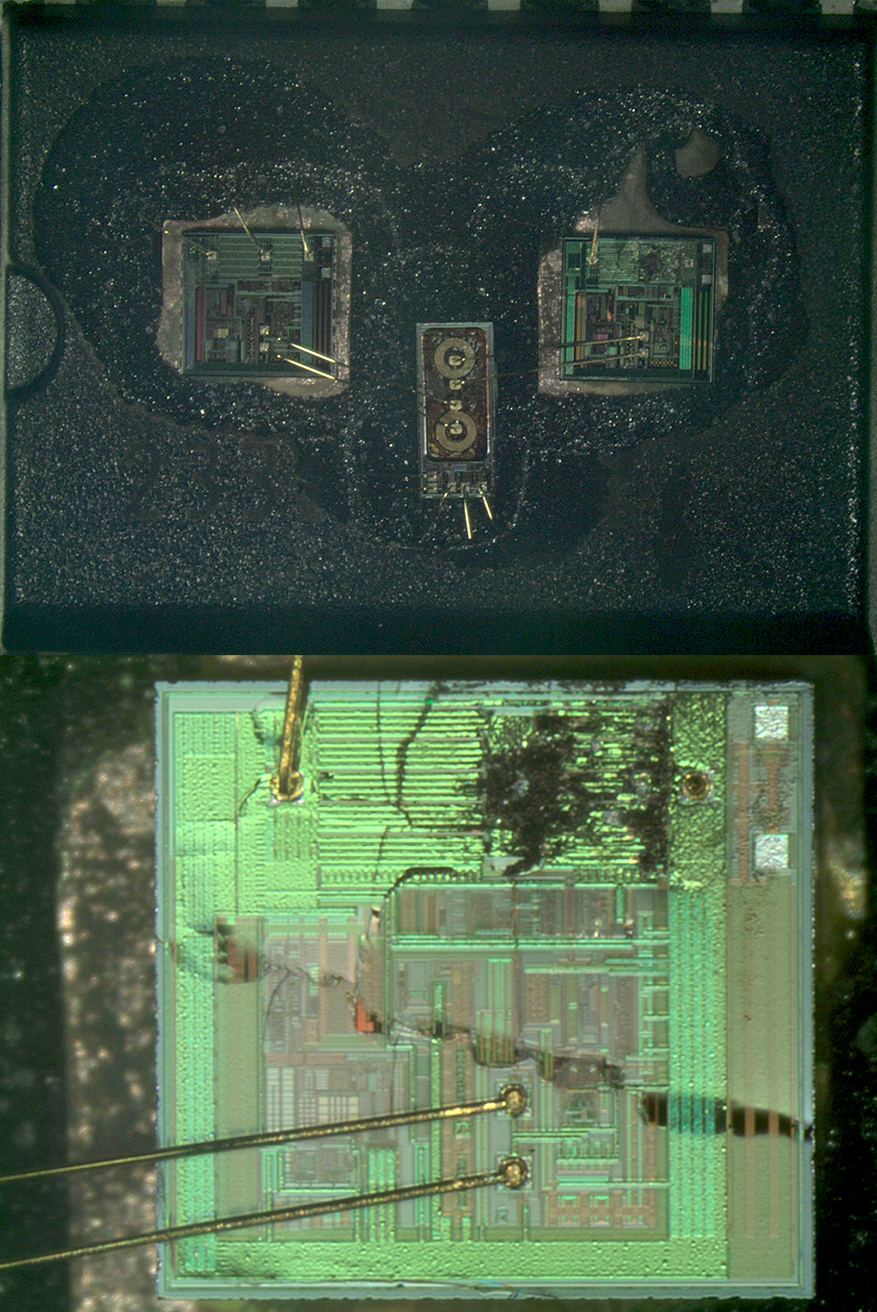
Partial encapsulation of gate drivers shows similar chip damages for different switches and different test conditions. Figure 8 shows the damage for a P-MOSFET based output driver stage in test 8 (Table 1). The test at a bulk voltage 750 V caused an IGBT explosion, as well as the destruction of limiting devices Rg and DZ; however, only a small molten area very close to the bond wire of pin VDDA is visible. The gate overcurrent during the damage phase flowed via the intrinsic diode of P-MOSFET into the 100 µF capacitor. Due to current crowding, the area close to the bond wire melted. No further driver chip damage and no isolation damage on the control chip was observed. Figure 9 shows molten areas during test 9, where a high voltage of 150 V was directly applied to the driver chip. The electrical isolation of the control chip survived this extreme overstress test.

Only the appearance of a small molten area on the output chip occurred. No damage of the isolation
was detected.

Extreme electrical overstress did not destroy the control chip. No damage of the isolation was detected.
The unlimited energy applied to the output driver destroyed the circuitry; remarkable molten area.
However, no damage of the isolation was observed.
The worst case on the primary side exhibits the application of excessive supply voltage to the control chip. Thus, in test 11, a supply voltage of 15 V was applied to the VDD1 pin (Figure 5), which significantly exceeds the absolute maximum rating of 7.0 V. The photo in Figure 11 shows molten areas in the chip in the vicinity of the VDD1 pin.
The energy applied to the circuit created a very limited molten region surrounding the VDD1 pin. No damage
of the isolation was observed.
Conclusion
Destructive tests of power switches do not impact the isolation withstand of the integrated gate driver ADuM4223/ADuM3223. Even if the driver was damaged due to an excess of energy flowing into the output chip, only local and limited molten areas occurred. The energy excess was directed via the P-MOS driver transistor into the blocking capacitors. Thus, the molten areas occurred in the P-MOS region only.
The chip arrangement of ADuM4223/ADuM3223 does not allow diffusion of molten areas into the control chip, which includes the galvanically isolated signal transformer. To limit the energy flowing into the driver output, a Zener diode can be used. The Zener diode in combination with an appropriate gate resistor can protect the gate driver during the power switch damage phase. It is possible to design the gate resistor to manage power dissipation during regular work and to separate the driver from the power switches during their destruction. When high voltage is directly applied into the chip, the gate resistor acts as a fuse. The resistor limits chip damage to small molten areas around the output power switch.
In the worst case, when unlimited energy was applied to the output chip, limited molten area in the vicinity of the driver’s output pin occurred. This test did not impact the isolation withstand. In the worst case on the primary side, when the supply voltage rose significantly above the absolute maximum rating, a limited molten area surrounding the supply voltage pin was observed. There was no sign of weakening of the isolation in any electrical overstress test. A high voltage isolation test, performed afterward, confirmed the withstand performance of the electrical microisolation. The appropriate chip construction, as well as the chip arrangement inside the driver package, avoided proliferation of the destructive energy into the high voltage isolation layer of the microtransformer.
References
1 Baoxing Chen and Bernhard Strzalkowski. “Isolated Gate Driver Using Microtransformers.” ECPE workshop “Electronica Around the Power Switches.” June 29, 2011.
2 Andreas Volke, Michael Hornkamp, and Bernhard Strzalkowski. “IGBT/MOSFET Applications Based on Coreless Transformer Driver IC 2ED020I12-F.” Proceedings of PCIM 2004, Nürnberg, 2004.
3 SLLA198. “The ISO72x Family of High Speed Digital Isolator.” Texas Instruments.
4 Bernhard Strzalkowski. “High Performance IGBT-Driver in Microtransformer Technology Providing Outstanding Insulation Capability.” Proceedings of PCIM2007, Nürnberg, 2007.
5 Bernhard Strzalkowski. “Maximum Power Limit for Withstand Insulation Capability of IGBT/MOSFET Gate Drivers.” Proceedings of PCIM 2014, 2014.
About the Author: Bernhard Strzalkowski studied electrical engineering at the Silesian University of Technology in Gliwice, Poland and Karlsruhe Institute of Technology in Germany, and received his Dipl.-Ing. degree in electrical engineering from Karlsruhe Institute of Technology in 1989. In 2003, he received a Ph.D. in electronics from Silesian University of Technology. From 1989 to 1996 he worked as a research and development engineer with Magnet-Motor in Starnberg developing power electronics for wind power converters and electrical/hybrid cars. From 1997 to 2008 he joined Siemens and Infineon in Munich, where his research and design work comprised integrated circuits for industrial and automotive applications. In February 2009, he joined Analog Devices in Munich, working on power management, digital power, and iCoupler applications. He supports automotive and communication infrastructure customers in Europe and has been granted numerous patents relating to the field of power electronics. He is a member of the standards committees ICE and VDE, as well as the PCIM advisory board. He can be reached at bernhard.strzalkowski@analog.com.
 If you enjoyed this article, you will like the following ones: don't miss them by subscribing to :