On Semi opens advanced sensor fusion design centers in EU
The first is an image sensor fusion design center in Bracknell, England. The team has more than 1,200 years of experience in silicon design, which implies a team of more than 30 engineers
On Semi is already a vendor of image sensors into industrial and automotive applications and acquired Truesense Inc., the image sensor arm of Kodak Corp. in 2014 (see On Semi buys former Kodak image sensor business). The Bracknell center is expected to add imaging and video signal processing for automated driving systems.
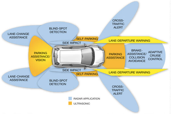
This will be combined with technology from a millimeter-wave radar design center in Haifa, Israel, that On Semi has announced it is acquiring from IBM. The combination will allow On Semi to address sensor fusion where multiple sensing technologies are used to improve accuracy and automotive safety.
The Haifa design centers includes staff, equipment, research facilities and intellectual property. The team has established E-band designs that meet the European ETSI standard.
Both design centers report into On Semi’s image sensor division.
News articles:
On Semi buys former Kodak image sensor business
Analog firm qualifies IP with On Semi
On Semi clear to buy Fairchild
 If you enjoyed this article, you will like the following ones: don't miss them by subscribing to :
eeNews on Google News


